
go to D & T type flip-flops
Latch and Flip-flop
Talking about sequential logic, we need some kind of memory to design a sequential circuit, along with the combinational logic. I don’t know who invented it, but there is a 1-bit latch, which is starting point of the sequential design and its circuit diagram is here-
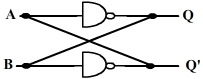
As we analyze the circuit, it is merely cross-connection of two inverters (because if both inputs of NAND are shorted, it’s inverter). Let’s say A and B are inputs and outputs are Q and Q’. A is connected to Q’ while B to Q. As the representation suggests, Q and Q’ are always complementary.
This circuit has 2 stable states
i) If Q = 0 then Q’ = 1; this is called RESET state
ii) If Q = 1 then Q’ = 0; termed as SET state
While circuit is in SET state, Q = B = 1 and hence Q’ = ~B = 0. (~ means negation). And since Q’ = A, Q = ~A = 1. So, the circuit continues to be in SET state. Since the output is latched forever, we call this circuit a LATCH. Same is true if latch is in RESET state.
But what decides the state in which latch is? And what if we want state to change from SET to RESET or vice versa? There should be some provision to give external inputs to the latch so that we can control its state.
Some modification to the above latch circuit is shown below-
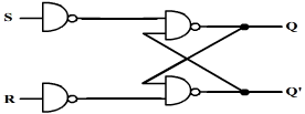
This is called a S-R latch where, S is SET and R is RESET. Inputs are so named because they decide the state of S-R latch.
Ok fine. The latch has got some memory and we put whatever bit (0 or 1) we want to put it in. But what makes it a ‘sequential’ circuit? It is a sequential circuit because its output does not merely depend on inputs but the sequence in which inputs are fed to it. This can be elaborated with the following table:
Ok fine. The latch has got some memory and we put whatever bit (0 or 1) we want to put it in. But what makes it a ‘sequential’ circuit? It is a sequential circuit because its output does not merely depend on inputs but the sequence in which inputs are fed to it. This can be elaborated with the following table:
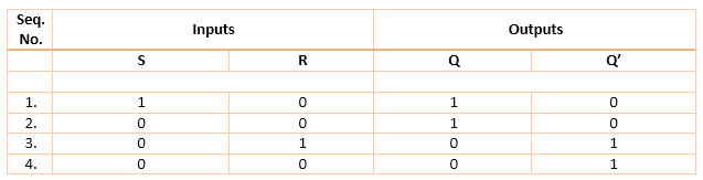
Seq. No. 1
S = 1, R = 0 is SET state. So, output Q is 1 and Q’ is 0.
Seq. No. 2
Both inputs are 0 i.e. excitation is removed. The SET state is latched.
Seq. No. 3
R = 1, S = 0 is RESET state; Q’ is 1 and Q is 0.
Seq. No. 4
Again excitation is removed. RESET state is latched.
For both Seq. No. 2 and Seq. No. 4, the input to the latch is same. However, the output of latch is not same but depends on previous input. The output is thus dependent on the sequence in which inputs are fed.
If inputs to the latch are S = R = 1, then the circuit behaves unpredictably, because both outputs. This state is known to be ‘not used’ or ‘prohibited’ state and not useful for any application.
Next modification to the latch is a ‘clocked latch’ aka flip-flop. The memory cell is set or reset in synchronism with a clock signal which train of pulses.
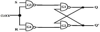
Truth table of S-R flip-flop is:
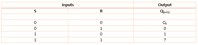
And Q’ = ~Q always, which is not shown in table above.
Whenever CLOCK = 1, SET or RESET inputs are latched into the memory cell and output is set or reset. When CLOCK = 0, gates G3 and G4 output logic 1 and hence the memory cell retains its current state. If CLOCK = 1, S = 1 and R = 1, then the output of flip-flop is unpredictable. Depending on gate delays (propagation delays) of G1 and G2, either SET or RESET state may occur. So, S=R=1 is ‘not used’ or ‘prohibited’ state for S-R flip-flop.
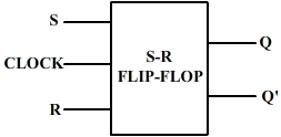
Logic symbol of S-R flip-flop.
Whenever CLOCK = 1, SET or RESET inputs are latched into the memory cell and output is set or reset. When CLOCK = 0, gates G3 and G4 output logic 1 and hence the memory cell retains its current state. If CLOCK = 1, S = 1 and R = 1, then the output of flip-flop is unpredictable. Depending on gate delays (propagation delays) of G1 and G2, either SET or RESET state may occur. So, S=R=1 is ‘not used’ or ‘prohibited’ state for S-R flip-flop.
Logic symbol of S-R flip-flop.
Further, two more inputs are generally available in S-R flip-flop, known as PRESET and CLEAR.
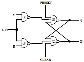
PRESET (PR) and CLEAR (CR) are active low inputs meaning that they are activated by logic 0 state.
PR = 1, CR = 1 leads to normal flip-flop operation as discussed earlier.
PR = 0, CR = 1 causes flip-flop to be in SET state irrespective of other inputs given.
PR = 1, CR = 0 causes flip-flop to be in RESET state irrespective of other inputs given.
PR = 0, CR = 0 leads to uncertain behavior and hence not used.
Logic symbol:
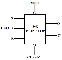
The bubbles on PRESET and CLEAR inputs indicate that they are active low signals. Logic symbols will be used further to eliminate complex connections.
J-K Flip-Flop
The drawback of S-R flip-flop is its uncertain state when both inputs are HIGH. To deal with this, it is further modified into a J-K flip-flop.
A twisted feedback is taken from the outputs to inputs as shown below
A twisted feedback is taken from the outputs to inputs as shown below

The same can be implemented without using extra AND gates. The feedback is given to three input NAND gates as shown below:

|

|
Truth table of J-K flip-flop:
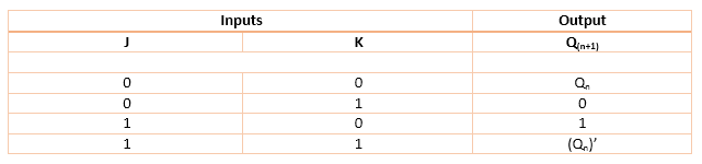
This is same as that of S-R flip-flop except for fourth row, where uncertainty is eliminated and output for condition J=K=1 at current clock pulse is complement of output at previous clock pulse. However, this output is not stable.
Race-Around condition:
Consider that J-K flip-flop is in RESET state i.e. Q = 0. Now that we apply J=K=1, output becomes complement to previous value i.e. now Q = 1. After the time interval equal to propagation delay of gates, the output is again complemented and becomes Q = 0. This continues as long as CLOCK = 1 and J=K=1. This phenomenon is termed as output races from 0 to 1 to 0 to 1 and so on . . .
This is called race-around condition.

Although the output of J-K flip-flop for fourth row is not uncertain, it is not useful either. The figure shows how output races between 0 and 1 as long as CLOCK is HIGH. When CLOCK goes LOW, whatever is the output is retained.
Master-Slave J-K Flip-Flop

The Master-Slave J-K flip-flop consists of two S-R flip-flops connected in cascade; one is called master and other one which follows master is slave. Master and slave are driven by same clock but out-of-phase. This means that when clock enables master, slave is not enabled and vice versa. The feedback is taken from outputs of slave to the inputs of master.
For CLOCK = 1,
Outputs QM and QM’ respond to the inputs. At this time, Q and Q’ are not disturbed because clock pulse for slave is low.
For CLOCK = 0,
Slave follows master and Q & Q’ depend on QM & QM’.
Since the outputs for each, master and slave, are changing at different intervals of time, the race around condition is avoided.
Logic symbol of M-S J-K Flip-Flop shows bubble at clock input, meaning that it is negative edge triggered.

go to D & T type flip-flops
Our app is now available on Google Play.
![]()
