
back to latches & flip-flops
We started from a 1-bit memory element called latch, clocked it to get S-R flip-flop which sets or resets as desired, then made it J-K flip-flop which eliminates uncertainty in fourth-row from S-R flip-flop’s truth table but introduces race-around. The master-slave J-K flip-flop finally gave us stable outputs for all possible input combinations. Now that we get stable outputs, still there is chance for some improvement.
The drawback, we can say, of M-S J-K flip-flop is that it need two inputs to be specified simultaneously to decide what output it gives. This is particularly problem for data storage like applications. Why give two inputs to store a single bit? Can we use one input only?
The drawback, we can say, of M-S J-K flip-flop is that it need two inputs to be specified simultaneously to decide what output it gives. This is particularly problem for data storage like applications. Why give two inputs to store a single bit? Can we use one input only?
D Flip-flop
If we want to store only a bit into a flip-flop, we give one input to it; a LOW input to store logic 0 and a HIGH input to store logic 1. This is possible if we use middle two rows of truth table of any of flip-flops so far discussed.
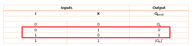
For these two rows (highlighted by red box), two inputs are complementary. So, we can connect them with an inverter in between. The common input is called ‘D’ which stands for Data input.

For D = 0, Q = 0
For D – 1, Q = 1 at the end of each clock pulse.
This means that output simply follows the input on each clock transition thereby introducing a time delay of a clock period between input and outputs. For this reason, this flip-flop is also called a Delay flip-flop.
Logic symbol:
For D – 1, Q = 1 at the end of each clock pulse.
This means that output simply follows the input on each clock transition thereby introducing a time delay of a clock period between input and outputs. For this reason, this flip-flop is also called a Delay flip-flop.
Logic symbol:

Our app is now available on Google Play.
![]()
T Flip-flop
Now we’ll use first and fourth row of the truth table of a J-K flip-flop.
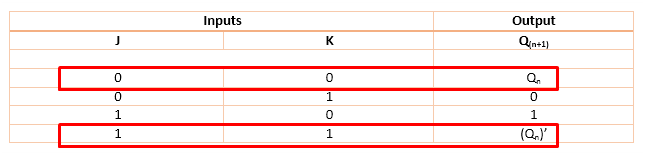
Here, both inputs are same, so we tie them together directly. When this common input is LOW, the output is retained. When input goes HIGH, the output toggles from its previous state. This is called a toggle flip-flop.
Since the flip-flop is ‘edge triggered’, the toggle occurs only once in a clock cycle. The output toggles when T = 1, and is retained otherwise.
Since the flip-flop is ‘edge triggered’, the toggle occurs only once in a clock cycle. The output toggles when T = 1, and is retained otherwise.

|

LOGIC SYMBOL
|
go to Registers
Our app is now available on Google Play.
![]()
