
|
Why memory access is important aspect? The statistics* obtained by running some program on ARM processor shows that, around 43% of instructions dynamically executed by the processor are related to the data transfer (to and from memory), while 23% of instructions are related to control flow i.e. to branch to a sub-routine. Only 34% are ALU instructions & other. Though this statistics are obtained for ARM, similar is case for almost all general-purpose computing applications. (* reference from book : Steve Furber, "Arm - System-on-chip architecture", 2nd ed, 2000) So, a processor, which is defined to be a digital thing that 'processes' data, indeed shows most of its performance in moving the data to and form memory. In this context, the memory access should definitely be considered while designing a processor. For what purpose does a processor access the memory? - to fetch an instruction - to fetch data operands from memory - to store data result in memory etc. The memory mentioned here is either its internal memory (registers) or the external memory connected to processor such as disk/sdCard etc. In case of internal memory, the access time is much low, but access time for external memory is often not negligible, given the fact that almost 40% time of program execution is spent on memory access. For various kinds of memories connected to a CPU, the speed and capacity hierarchy is as shown in figure below: 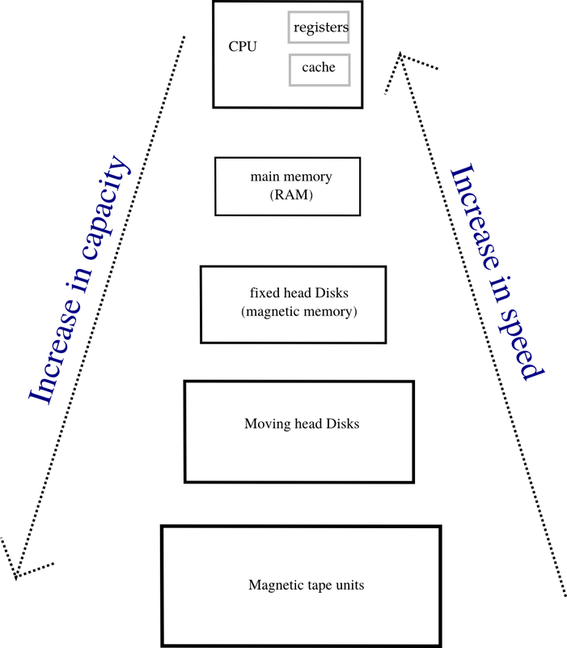
Since the registers are available on-chip, their access time is lowest. The main memory (RAM) is frequently accessed by CPU, which is comparatively slower. Thus, a secondary on-chip memory, called CACHE memory is often used in modern processors. The cache stores some data/code which is frequently needed. Connect with Digital Byte on facebook to get updates.
0 Comments
From the instruction set of MU0, it may seem like the ALU needs to perform only two operations viz. ADD and SUB. However, the way the datapath is designed, ALU gets some additional responsibilities.
Consider that X and Y are LHS and RHS inputs to ALU respectively, and Z is its output. X bus is accessed by ACC and PC, while Y bus accessed by IR and memory. The RTL (Register-Transfer Level) datapath is sketched so as to ensure that every desired operation can be performed. In other words, the datapath is so sketched that internal signals get all necessary paths from register-to-register.
|
The Digital Byte App.
Like facebook page to get updates :
ArchivesCategories
All
|
 RSS Feed
