
|
From the instruction set of MU0, it may seem like the ALU needs to perform only two operations viz. ADD and SUB. However, the way the datapath is designed, ALU gets some additional responsibilities. Consider that X and Y are LHS and RHS inputs to ALU respectively, and Z is its output. X bus is accessed by ACC and PC, while Y bus accessed by IR and memory. 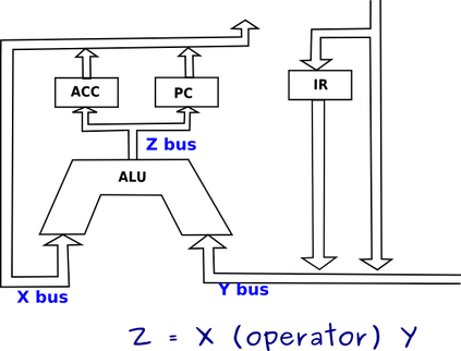 Following are the operations supported by MU0 ALU: 1) Addition (ADD instruction) Z = X+Y where, X = [ACC] and Y = [memory] 2) Subtraction (SUB instruction) Z = X-Y. In this case, the adder can act as subtractor. The ALU performs Z = X+(-Y) where, X = [ACC] and Y = [memory] 3) Increment PC After each and every instruction, the PC is incremented by 1. The ALU performs Z = X + 1 where X = [PC] 4) Write to ACC (LDA instruction) and to PC (branch instruction) The ALU performs Z = 0 + Y where Y = [IR] Each operation can be expressed as an addition operation. This means that ALU contains ADDER and other circuitry to choose the proper operand. The MU0 ALU schematic :  Pre-condition logic is able to reset either of the operands to 0. For various operations, the pre-condition on X-bus and Y-bus, and carry-in are shown below in tabular form:
In conclusion, we can say that an adder, along with some extra logic is used to create this simple ALU. We'll stop this discussion on MU0 processor here. Next is what? . . . let's discuss next the things that makes a processor more powerful... Connect with Digital Byte on facebook to get updates.
0 Comments
Leave a Reply. |
The Digital Byte App.
Like facebook page to get updates :
ArchivesCategories
All
|
 RSS Feed
